In semiconductor fabrication, gases do all the work and lasers get all the attention. While lasers do etch transistor patterns into silicon, the etch that first deposits the silicon and breaks down the laser to make complete circuits is a series of gases. It is not surprising that these gases, which are used to develop microprocessors through a multi-stage process, are of high purity. In addition to this limitation, many of them have other concerns and limitations. Some of the gases are cryogenic, others are corrosive, and still others are highly toxic.
All in all, these limitations make manufacturing gas distribution systems for the semiconductor industry a considerable challenge. Material specifications are demanding. In addition to material specifications, a gas distribution array is a complex electromechanical array of interconnected systems. The environments in which they are assembled are complex and overlapping. Final fabrication takes place on site as part of the installation process. Orbital soldering helps meet the high specifications of gas distribution requirements while making manufacturing in tight, challenging environments more manageable.
How the semiconductor industry uses gases
Before attempting to plan the manufacture of a gas distribution system, it is necessary to understand at least the basics of semiconductor manufacturing. At its core, semiconductors use gases to deposit near-elemental solids on a surface in a highly controlled manner. These deposited solids are then modified by introducing additional gases, lasers, chemical etchants, and heat. The steps in the broad process are:
Deposition: This is the process of creating the initial silicon wafer. Silicon precursor gases are pumped into a vacuum deposition chamber and form thin silicon wafers through chemical or physical interactions.
Photolithography: The photo section refers to lasers. In the higher extreme ultraviolet lithography (EUV) spectrum used to make the highest specification chips, a carbon dioxide laser is used to etch the microprocessor circuitry into the wafer.
Etching: During the etching process, halogen-carbon gas is pumped into the chamber to activate and dissolve selected materials in the silicon substrate. This process effectively engraves the laser-printed circuitry onto the substrate.
Doping: This is an additional step that changes the conductivity of the etched surface to determine the exact conditions under which the semiconductor conducts.
Annealing: In this process, reactions between wafer layers are triggered by elevated pressure and temperature. Essentially, it finalizes the results of the previous process and creates the finalized processor in the wafer.
Chamber and Line Cleaning: The gases used in the previous steps, especially etching and doping, are often highly toxic and reactive. Therefore, the process chamber and the gas lines feeding it need to be filled with neutralizing gases to reduce or eliminate harmful reactions, and then filled with inert gases to prevent the intrusion of any contaminating gases from the outside environment.
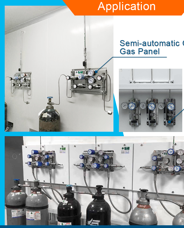
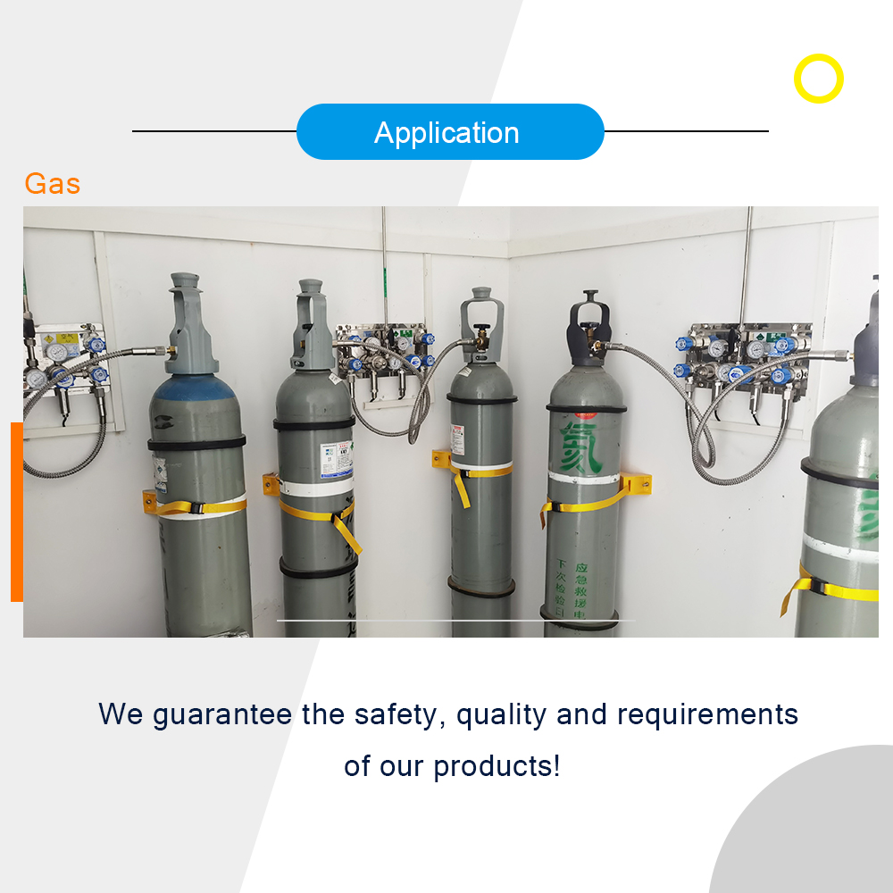
Gas distribution systems in the semiconductor industry are often complex because of the many different gases involved and the tight control of gas flow, temperature and pressure that must be maintained over time. This is further complicated by the ultra-high purity required for each gas in the process. The gases used in the previous step must be flushed out of the lines and chambers or otherwise neutralized before the next step of the process can begin. This means that there are a large number of specialized lines, interfaces between the welded tube system and the hoses, interfaces between the hoses and tubes and the gas regulators and sensors, and interfaces between all of the previously mentioned components and the valves and sealing systems designed to prevent pipeline contamination of the natural gas supply from being swapped out.
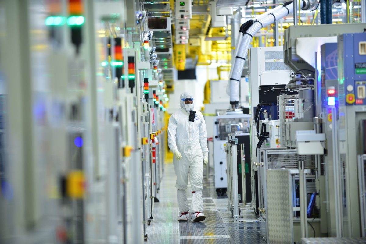
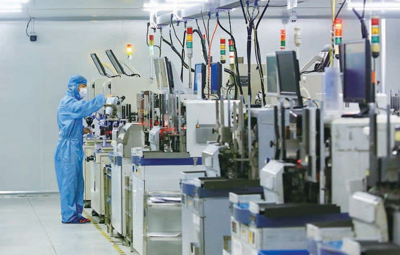
In addition, cleanroom exteriors and specialty gases will be equipped with bulk gas supply systems in cleanroom environments and specialized confined areas to mitigate any hazards in the event of accidental leakage. Welding these gas systems in such a complex environment is no easy task. However, with care, attention to detail and the right equipment, this task can be accomplished successfully.
Manufacturing gas distribution systems in the semiconductor industry
The materials used in semiconductor gas distribution systems are highly variable. They can include things like PTFE-lined metal pipes and hoses to resist highly corrosive gases. The most common material used for general purpose piping in the semiconductor industry is 316L stainless steel – a low carbon stainless steel variant. When it comes to 316L versus 316, 316L is more resistant to intergranular corrosion. This is an important consideration when dealing with a range of highly reactive and potentially volatile gases that can corrode carbon. Welding 316L stainless steel releases less carbon precipitates. It also reduces the potential for grain boundary erosion, which can lead to pitting corrosion in welds and heat affected zones.
To reduce the possibility of piping corrosion leading to product line corrosion and contamination, 316L stainless steel welded with pure argon shielding gas and tungsten gas shielded weld rails is the standard in the semiconductor industry. The only welding process that provides the control needed to maintain a high purity environment in process piping. Automated orbital welding is only available in semiconductor gas distribution
Post time: Jul-18-2023