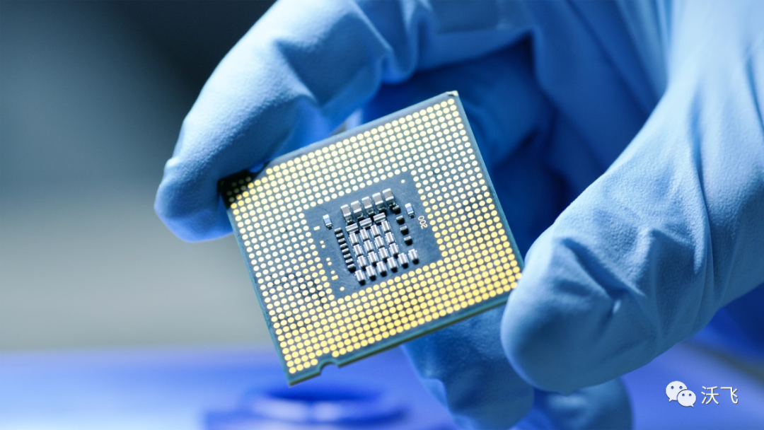
Ultra-high purity gases are essential throughout the semiconductor supply chain. In fact, for a typical fab, high-purity gases are the largest material expense after silicon itself. In the wake of the global chip shortage, the industry is expanding faster than ever – and the demand for high purity gases is increasing.
The most commonly used bulk gases in semiconductor manufacturing are nitrogen, helium, hydrogen and argon.
Nitrogen
Nitrogen makes up 78% of our atmosphere and is extremely abundant. It also happens to be chemically inert and non-conductive. As a result, nitrogen has found its way into a number of industries as a cost-effective inert gas.
The semiconductor industry is a major consumer of nitrogen. A modern semiconductor manufacturing plant is expected to use up to 50,000 cubic meters of nitrogen per hour. In semiconductor manufacturing, nitrogen acts as a general purpose inerting and purging gas, protecting sensitive silicon wafers from reactive oxygen and moisture in the air.
Helium
Helium is an inert gas. This means that, like nitrogen, helium is chemically inert – but it also has the added advantage of high thermal conductivity. This is particularly useful in semiconductor manufacturing, allowing it to efficiently conduct heat away from high-energy processes and help protect them from thermal damage and unwanted chemical reactions.
Hydrogen
Hydrogen is used extensively throughout the electronics manufacturing process, and semiconductor production is no exception. In particular, hydrogen is used for:
Annealing: Silicon wafers are typically heated to high temperatures and slowly cooled to repair (anneal) the crystal structure. Hydrogen is used to transfer heat evenly to the wafer and to assist in rebuilding the crystal structure.
Epitaxy: Ultra-high purity hydrogen is used as a reducing agent in the epitaxial deposition of semiconductor materials such as silicon and germanium.
Deposition: Hydrogen can be doped into silicon films to make their atomic structure more disordered, helping to increase resistivity.
Plasma Cleaning: Hydrogen plasma is particularly effective in removing tin contamination from light sources used in UV lithography.
Argon
Argon is another noble gas, so it exhibits the same low reactivity as nitrogen and helium. However, argon’s low ionization energy makes it useful in semiconductor applications. Because of its relative ease of ionization, argon is commonly used as the primary plasma gas for etch and deposition reactions in semiconductor manufacturing. In addition to this, argon is also used in excimer lasers for UV lithography.
Why purity matters
Typically, advances in semiconductor technology have been achieved through size scaling, and the new generation of semiconductor technology is characterized by smaller feature sizes. This yields multiple benefits: more transistors in a given volume, improved currents, lower power consumption and faster switching.
However, as the critical size decreases, semiconductor devices become increasingly sophisticated. In a world where the position of individual atoms matters, fault tolerance thresholds are very tight. As a result, modern semiconductor processes require process gases with the highest possible purity.
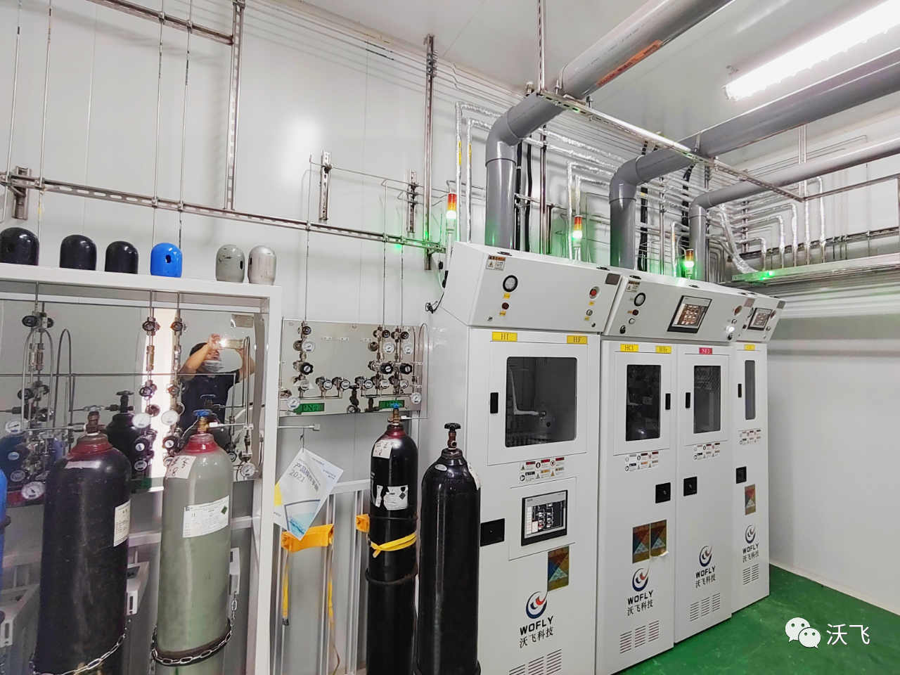
WOFLY is a high-tech enterprise specializing in gas application system engineering: electronic special gas system, laboratory gas circuit system, industrial centralized gas supply system, bulk gas (liquid) system, high purity gas and special process gas secondary piping system, chemical delivery system, pure water system to provide a full set of engineering and technical services and ancillary products from the technical consulting, overall planning, system design, selecting the equipment, prefabricated components, the installation and construction of the project site, the overall system testing, maintenance and other supporting products in an integrated manner.
Post time: Jul-11-2023